
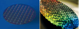
Patterned Test Wafer (Patterned wafer)
Semiconductor chip and device has reached to extreme level of industrial use, health science and other application. The world of semiconductor is becoming very dynamic and never ending technology is coming out day by day. Here, Advantec support for the varieties of pattern wafers by using multiple tools masks that fits to the application.
Pattern Wafer Products
|
Cu CMP Evaluation wafers  |
size | 300mm |
| Construction | Anneal / Cu EP 7KA Fill / Cu seed 1K / TaN 250A / Etch 3K (100nm Trench) / TEOS 3K / Si |
|
W CMP Evaluation wafers
|
size | 300mm |
| Construction | W 3K ~ 8K Fill / Ti: 150A / TiN: 150A Etch 3K ~ 8K / (130nm Via) PE-TEOS 2K / Si |
|
STI CMP Evaluation wafers
|
size | 300mm |
| Construction | HDP 6K Fill / Si etch 3.5K (130nm Trench) SiN 2K / Pad Ox 100A / Si |
|
TSV(Through Silicon Via) Wafer
|
size | 300mm |
| Construction | EP Cu 60um Fill / Cu seed 2um / TaN 600A / PE-TEOS 6K / Si Via etch 50um / Si |
|
Deep Si Etch(50um) via Wafer
|
size | 300mm |
| Construction | Si Via etch 50um / Si |
|
Double Patterning Wafer
|
size | 300mm |
| Construction | Etch (30nm Trench) 300A Poly Si +/- 5% 20A Sac Ox / S |


